GlobalFoundries Unveils 7nm-Class FDX Fusion Node: Evaluating Manufacturing Viability and Single-Die Integration for Edge AI and Automotive Architectures
当初の公開名: GlobalFoundries unveils 7nm-class FDX Fusion node — comes 7 years after firm abandoned FinFET
AI 概要
GlobalFoundries' 7nm FDX Fusion node offers hardware teams a potential single-die integration path for edge AI and automotive designs, though long-term adoption depends on upcoming PDK maturity and ecosystem readiness ahead of its 2028 production target.
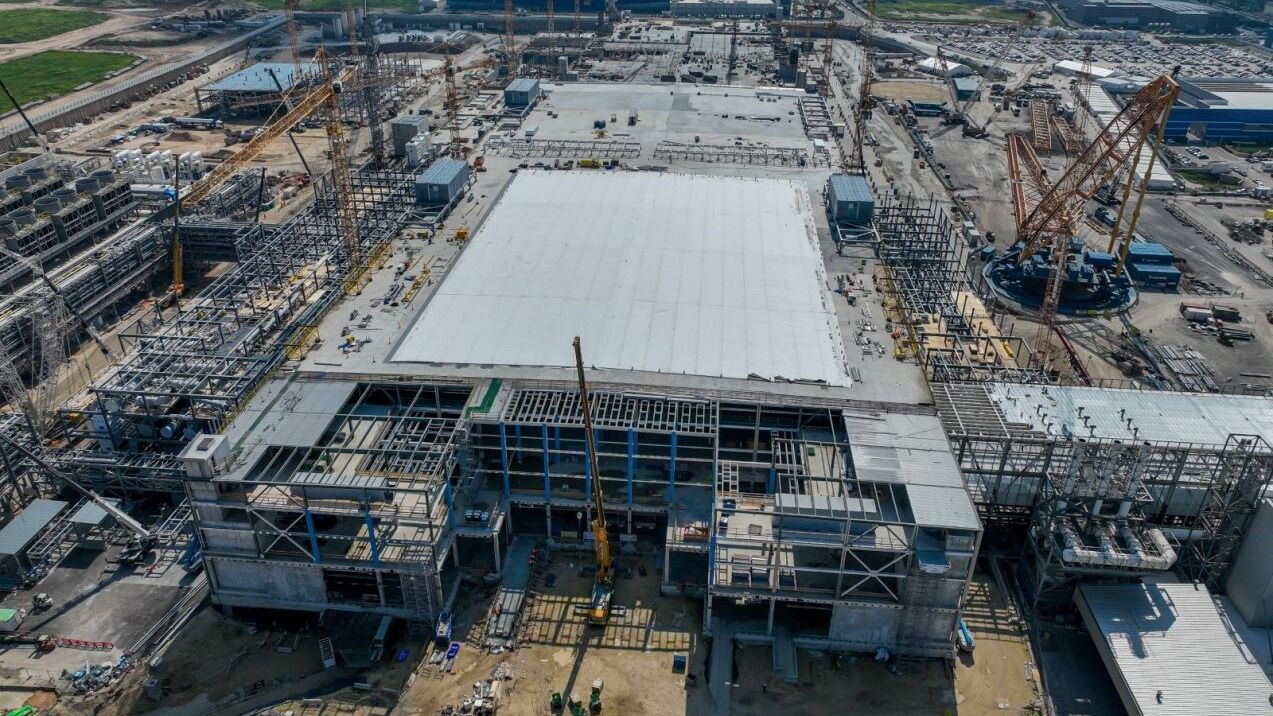
GlobalFoundries has unveiled FDX Fusion, a 7nm-class fully-depleted silicon-on-insulator (FD-SOI) manufacturing process slated for production at its Dresden, facility by 2028. This move comes roughly eight years after the foundry abandoned its 7nm FinFET roadmap, pivoting instead toward scaling planar FD-SOI technology to more than double the transistor density of its legacy 22FDX process while integrating high-frequency RF transistors up to 0.5 THz.
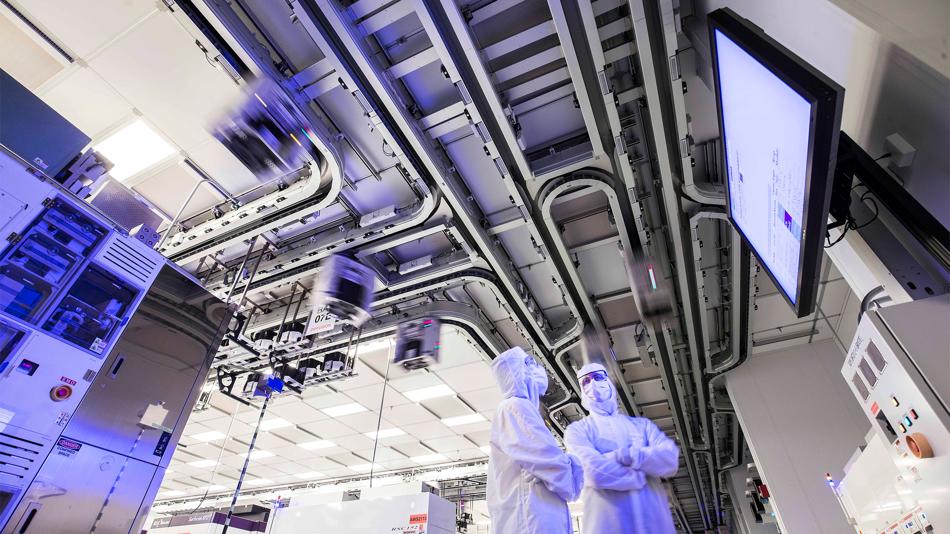
For hardware engineering teams, FDX Fusion targets applications that traditionally require multiple discrete dies, such as edge AI inference accelerators, automotive radar, and wireless communications systems. By combining digital logic with rich analog, mixed-signal, embedded nonvolatile memory, and in-memory computing options on a single die, the node aims to streamline system architectures, lower total power consumption, and eliminate multi-chip tapeout overhead.
Early industry engagement includes major automotive and industrial players like Infineon, Bosch, NXP, and Tesla, with initial demo silicon expected in early 2027 and process design kits (PDKs) arriving by mid-2027. However, because GlobalFoundries has yet to disclose explicit metrics like contacted gate pitch or detailed EDA ecosystem support, architectural adoption will depend heavily on upcoming PDK maturity and verified silicon performance benchmarks.
質問と回答
FDX Fusion is a 7nm-class fully-depleted silicon-on-insulator (FD-SOI) manufacturing process designed to combine high-density digital logic with RF, analog circuitry, and embedded memory on a single chip.