.avif)
.avif)
.avif)
.avif)
.avif)
Photograph the board or a region
Capture the area that matters — a bulging capacitor, a cluster of ICs, or a zoomed silk-screen. Phone photos are fine when text stays readable.
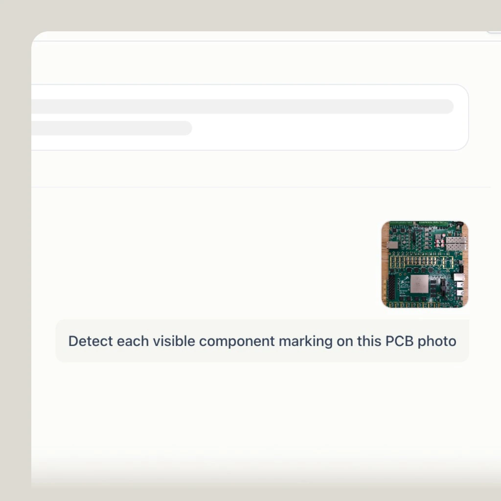

PCB Photo Part Identifier
Upload a board or zoomed region photo. PartGenie focuses on readable markings and printed parameters first — ideal for repair, reverse engineering, and on-site troubleshooting.
Drop a PCB photo here
Whole board or a close-up region. We’ll list readable markings and candidate MPNs in chat.
PNG / JPG / WebP · Max 25 MB · Readable areas first


















Capture the area that matters — a bulging capacitor, a cluster of ICs, or a zoomed silk-screen. Phone photos are fine when text stays readable.
PartGenie lists visible IC marks, printed passive ratings when present, and other readable labels. Unmarked MLCC values cannot be guaranteed from a photo alone.
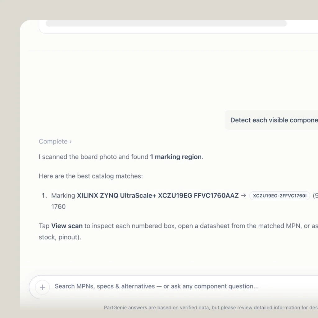
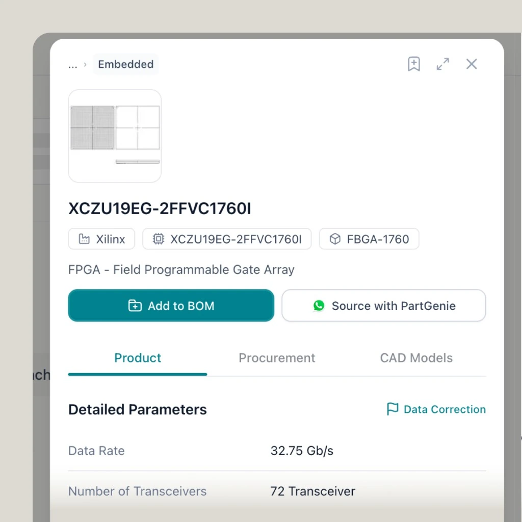
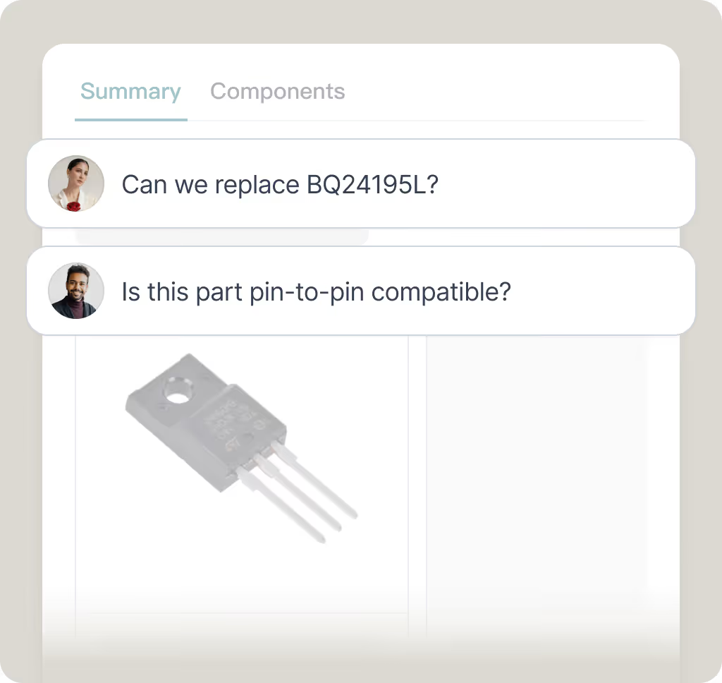
Use chat to open datasheets, decode clearer marks, or move into Alternative Finder once you have an MPN or replacement intent.
Use Cases
This page is a visual entry for PCB photos. It is not a full automated BOM extractor.
Top marks and package text when the photo is sharp enough.
Electrolytic labels and similar printed values when legible.
Unmarked MLCC capacitance, heavy glare, and dense whole-board BOM precision are out of scope for a single phone photo.
Continue to datasheet Q&A or Alternative Finder once MPNs are known.
“This is a game changer for electronics professional. The BOM feature was the best!”

“PartGenie precisely analyzes my customers' complex needs and instantly generates complete, viable hardware solutions. This analytical power, coupled with its ability to suggest a preliminary BOM, saves me days of work.”

Upload a PCB photo and continue in PartGenie chat.