
China Advances DUV Chipmaking Without EUV at Great Economic Cost: Manufacturing Analysis
Originally published as: China can make advanced chips without EUV, but the bill keeps growing
AI overview
Hardware engineering teams must weigh the cost and yield penalties of multi-patterned DUV silicon against traditional leading-edge nodes when assessing long-term component pricing and availability.
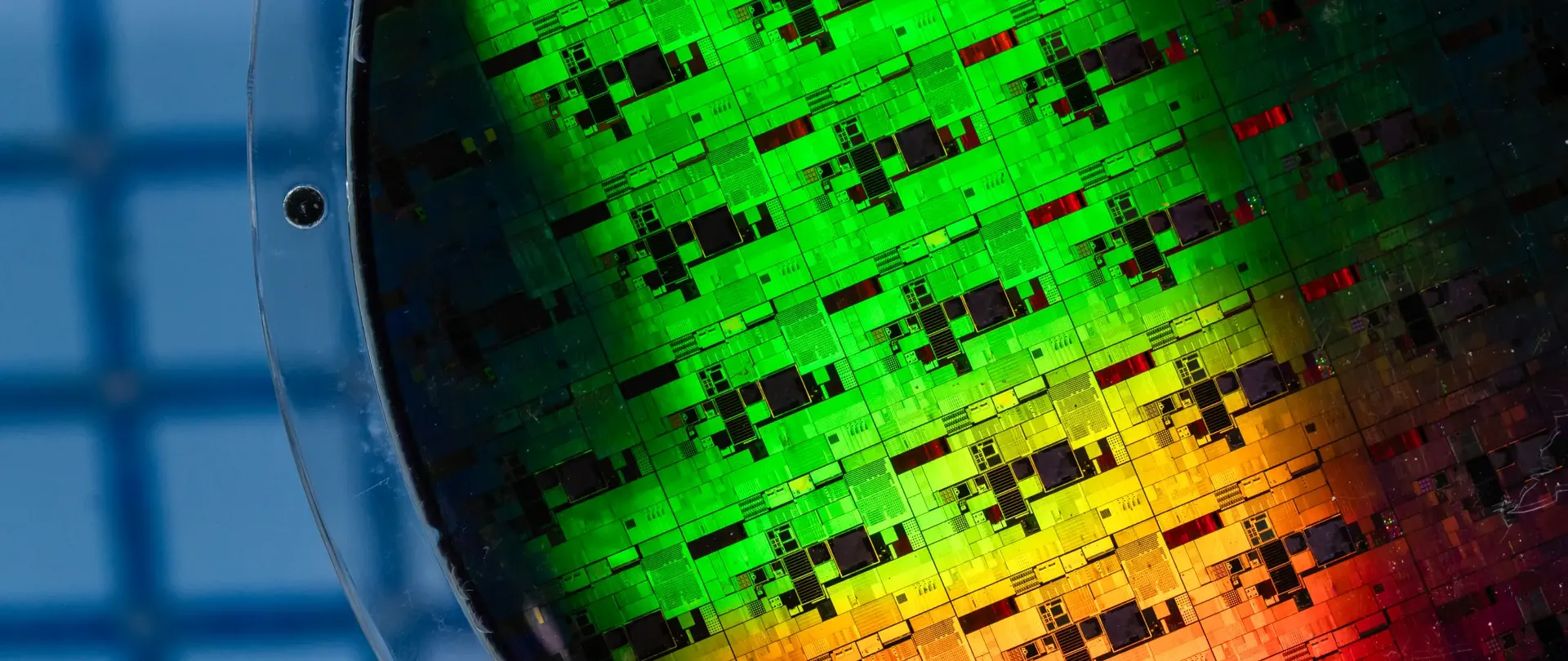
Export restrictions blocking ASML's extreme ultraviolet (EUV) systems have forced Chinese foundries like SMIC and memory makers like CXMT to heavily rely on deep ultraviolet (DUV) immersion lithography. By deploying complex multi-patterning techniques, local manufacturers have managed to produce processors resembling 7nm and 5nm-class densities. However, experts note that while technically feasible, bypassing EUV demands extraordinary trade-offs in manufacturing efficiency.
As the number of required masks increases beyond three exposures, the cumulative impact of overlay errors, process variations, and defect densities degrades wafer yields. To compensate for these variations, design teams must often loosen layout rules, resulting in significantly larger die sizes and fewer working dice per wafer. Consequently, while output volume can be artificially expanded through massive greenfield fab investments, the underlying economic and operational costs scale dramatically compared to single-pass EUV flows.
Hardware teams evaluating supply chains dependent on non-EUV nodes must factor in higher unit costs, potential yield volatility, and structural density gaps relative to TSMC or Samsung benchmarks. While memory architectures like 1-alpha DRAM demonstrate that DUV can be stretched successfully under specific conditions, advanced logic scaling past 3nm without EUV remains economically prohibitive.
Questions & answers
Yes, manufacturers can utilize deep ultraviolet (DUV) lithography combined with multiple patterning to produce advanced nodes, though at the expense of higher costs, lower yields, and larger die sizes.
