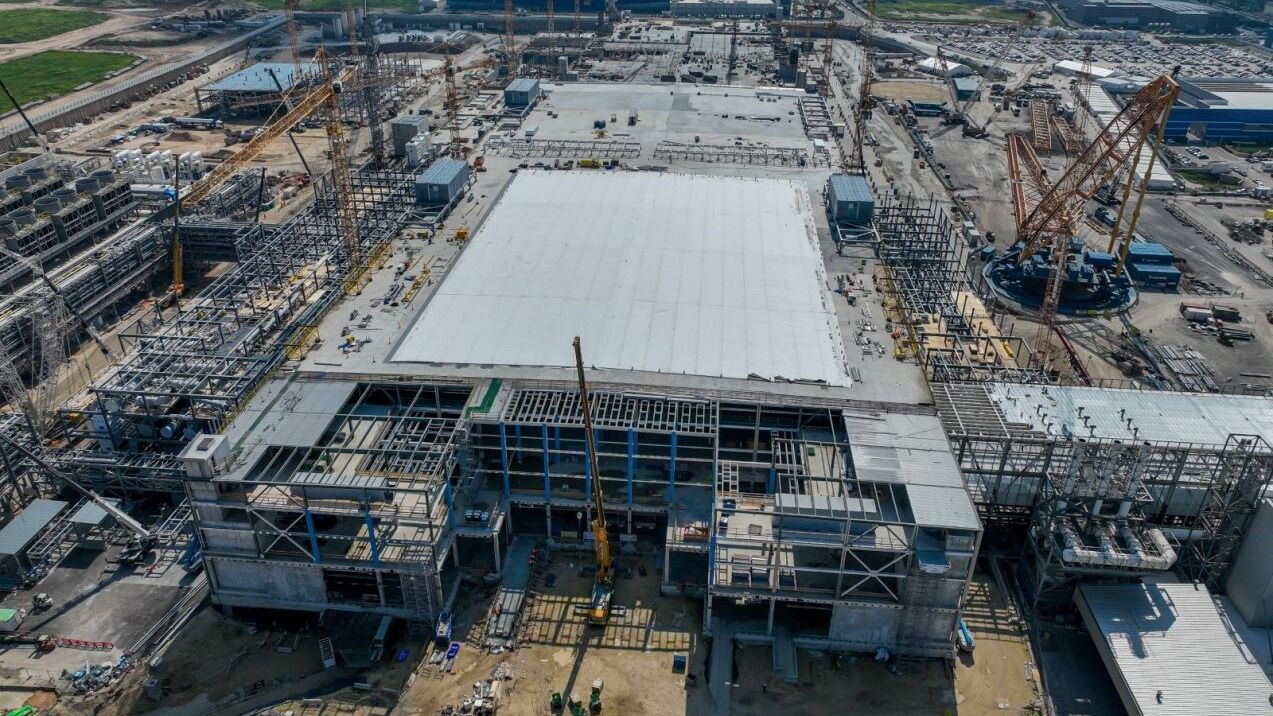
Applied Materials Opens $5B EPIC Center to Accelerate Advanced Chip Manufacturing
Originally published as: Applied Materials Bets $5B on a New Model for Chip Innovation

AI overview
Accelerated semiconductor R&D cycles at the EPIC Center will dictate future component roadmaps, node migration timelines, and availability for next-generation AI silicon.
Applied Materials has officially opened its Equipment and Process Innovation and Commercialization (EPIC) Center in Silicon Valley, marking a $5 billion commitment to fundamentally change how semiconductor equipment and process technologies are developed. Facing intense market pressures driven by artificial intelligence workloads, the facility is designed to bridge the gap between early-stage academic research and high-volume manufacturing. Major chipmakers and foundries, including TSMC and Samsung, have signed on as foundational partners to collaborate directly under one roof.
For hardware engineers and procurement teams, this collaborative model targets the scaling walls currently limiting next-generation architectures, such as thermal dissipation in dense 3D structures and performance bottlenecks in high-bandwidth memory. By compressing the timeline required to take atomic-scale materials, advanced patterning, and specialized etch processes from lab benches to production lines, the center aims to shorten future component lead times and smooth out technology node transitions.
Hardware teams should monitor how quickly these joint R&D cycles translate into pilot-line wafer runs and commercial PDK releases. While the facility promises faster introduction of high-performance compute nodes, success will ultimately depend on how effectively competing semiconductor giants can share foundational infrastructure without compromising proprietary intellectual property.
Questions & answers
It is a $5 billion collaborative research and development facility located in Silicon Valley designed to accelerate semiconductor equipment and process technology innovation.