
It is a composite semiconductor device containing one PNP epitaxial planar silicon transistor and one N-channel MOSFET in a single DFN-6L (2x2) package.
PNMT6N2 AI Analysis:
Datasheet, Specs, Alternatives & ECAD
AI summary
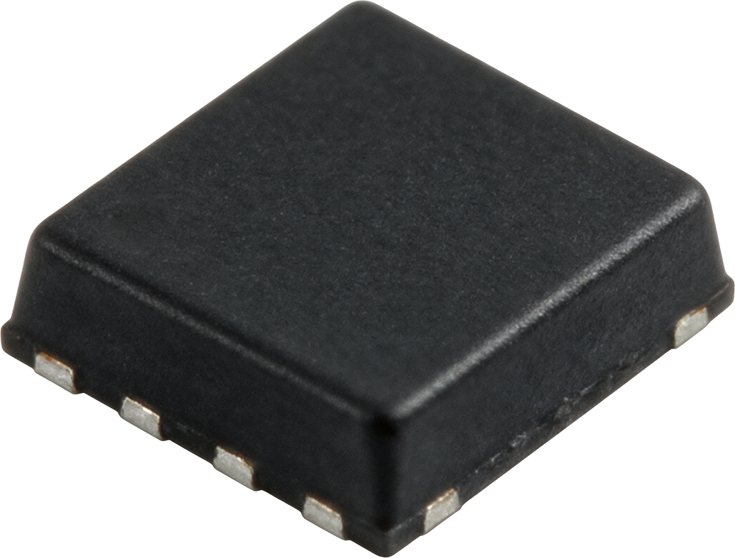
PNMT6N2
Transistors - FET
Key specifications
- Transistor IC
- 3 A
- MOSFET VDS
- 40 V
- Package
- DFN-6L (2x2)
Compliance & Environment
- RoHS
- Compliant
- REACH
- -
- MSL
- -
- ECCN
- -
- HTSUS
- -
Application
Power ManagementGeneral Switching
Datasheet
CAD Models
Download ECAD models for PNMT6N2: KiCad symbol & footprint, Altium footprint, PCB footprint, and 3D model.
EDA Symbol
Schematic symbol for your EDA tool
PCB Footprint
Land pattern for PCB layout
3D Model
STEP file for mechanical design
KiCad Library
Verified KiCad 8 symbol, footprint, and 3D model
Alternative components
Alternatives are being enriched. Analyze this part in PartGenie for the latest matches.